Links:https://www.i-micronews.com/products/glass-substrate-manufac ...
自華光電代理 全球第一大玻璃晶圓切割拋光廠商(計劃光學 PX)
對於半導體產業,玻璃材料通常提供兩種格式(晶圓和面板)和兩種密度(薄和厚)。此外,玻璃材料可以通過兩種方式來製造一款半導體元件產品:
* 玻璃基礎產品,玻璃材料被應用為一種永久性材料,並保留在最終產品中。
* 非玻璃基礎產品,玻璃基板僅短暫應用於製造流程中,IC元件加工完成後即去除。在這類產品中,玻璃作為載具功能用於元件的製造,但是不留存於最終產品中。
半導體玻璃材料市場集中於不同類別的玻璃材料供應商:
* 原材料製造商,如Schott、Corning以及AGC等,提供玻璃原材料、玻璃晶圓或玻璃面板。這些公司擁有有限的玻璃晶圓加工能力。
* 玻璃加工和結構化玻璃基板製造商,如PlanOptik,它們能夠對原材料供應商提供的原材料進行加工獲得圖型化和結構化的玻璃晶圓。這些公司通常從玻璃原材料供應商購買玻璃面板,然後由原材料設計/製造客戶的指定產品。
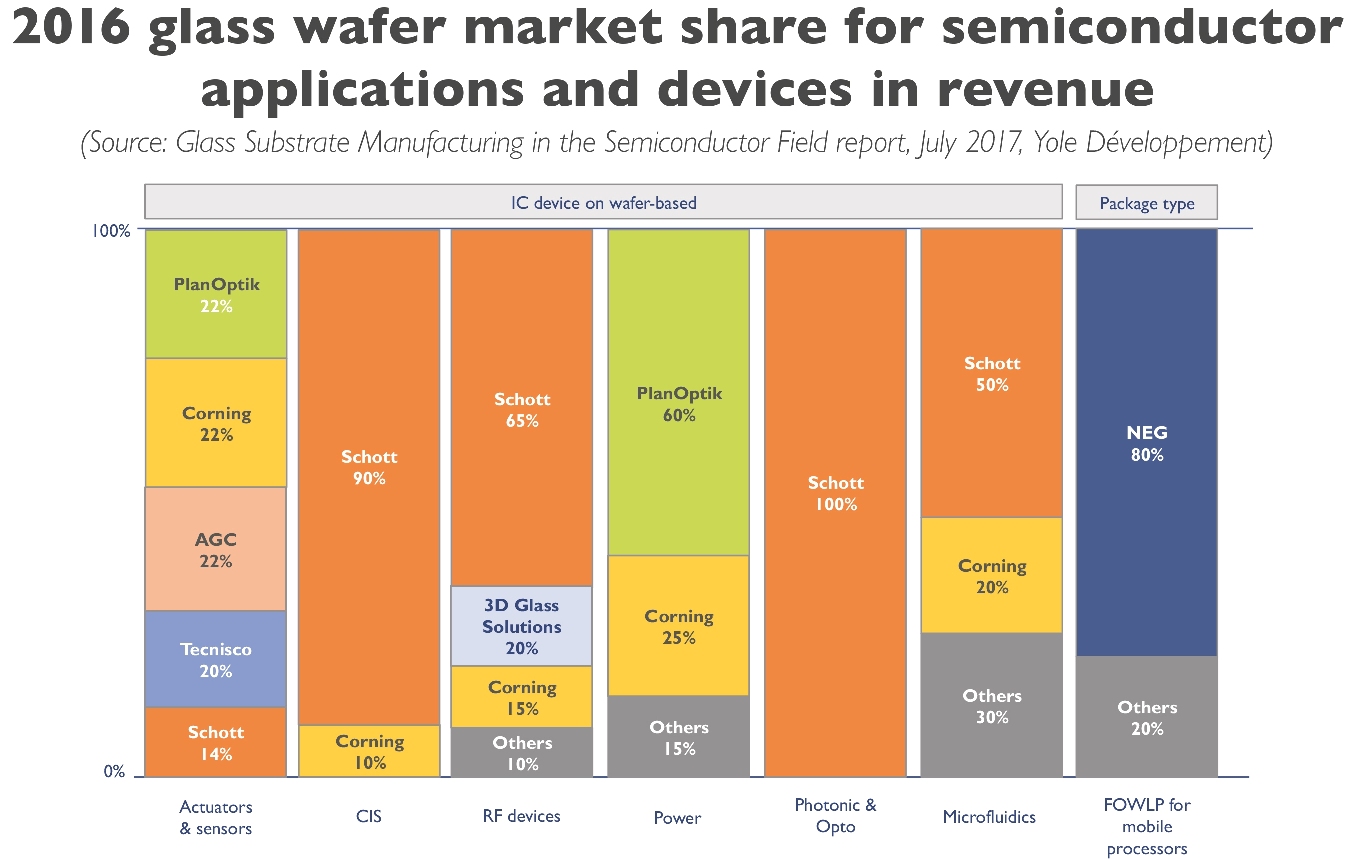
資料來源: Glass Substrate Manufacturing in the Semiconductor Field report – Yole Developpement - July 2017

自華光電 - 德國 計劃光學股份有限公司(PX, Plan Optik AG) 玻璃晶圓/石英晶圓/載體晶圓/矽玻璃晶圓 台灣/大陸獨家代理商。
Allen K. Lin | Allen@myblossom.tw | LINE ID: Allen-007 | Wechat ID: Allen-006 | T: 0910-782775
Glass Substrate Manufacturing in the Semiconductor Field report – Yole Developpement - July 2017
Specific to semiconductors, glass material is typically developed in two formats wafer and panel, and is available in two densities, thin and thick.
Moreover, glass material can be used in two different ways to fabricate a semiconductor device's product:
* Glass-based product where the glass material is applied as a permanent material and remains in the final product.
* A non-glass-based product where the glass substrate is only applied for temporary use in the process flow and then removed after the IC device is processed.
The glass material market for semiconductor is concentrated amongst glass material suppliers from different categories:
The glass material market for semiconductor is concentrated amongst glass material suppliers from different categories:
* Raw material manufacturers like Schott, Corning, and AGC providing raw glass material and blank wafers or sheets. These companies have limited wafer-processing capabilities.
* Glass processors and structured substrate manufacturers like PlanOptik, which can pattern and structure glass wafers from the raw material provided by raw material suppliers. These companies typically purchase wafers from raw-glass material suppliers and then design/create products from the raw material.
** Glass Wafer Materials
Schott: D263T eco , AF32 eco , MEMpax , BOROFLOAT 33 , B270 , FOTURAN II , AS87 eco , 0787 , BF33 , D263
Corning: SG3.4 , SG7.8 , SG9.0 , SG-HS , SG-HC , Eagle XG , EXG , EagleXG , SG 3.4
NEG: ABC-G , A58 , A66S , A69 , A75 , A91S
AGC: EN-A1
** Glass Wafer Materials
Schott: D263T eco , AF32 eco , MEMpax , BOROFLOAT 33 , B270 , FOTURAN II , AS87 eco , 0787 , BF33 , D263
Corning: SG3.4 , SG7.8 , SG9.0 , SG-HS , SG-HC , Eagle XG , EXG , EagleXG , SG 3.4
NEG: ABC-G , A58 , A66S , A69 , A75 , A91S
AGC: EN-A1