Links:http://www.planoptik.com/cnt/products/carrier_wafers.html

myBlossom Semiconductor Glass Wafers
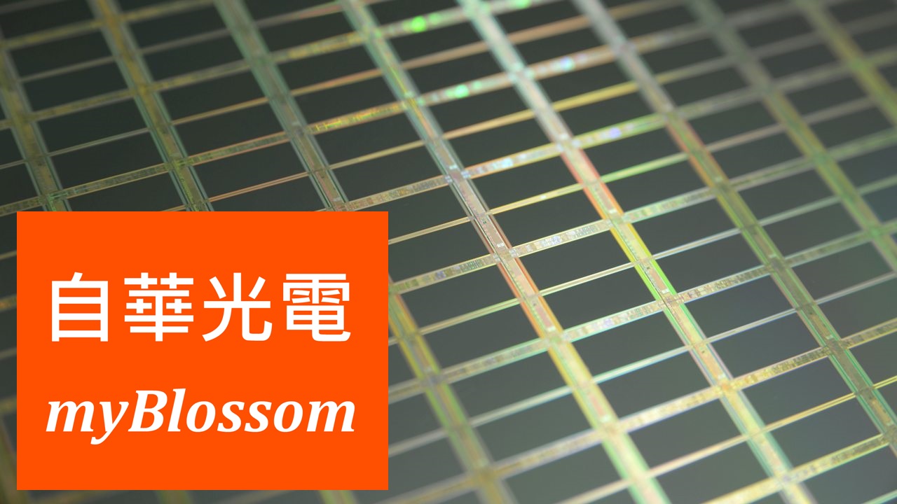
載具晶圓/載具玻璃晶圓 Glass Carrier Wafer
載體晶圓/載體玻璃晶圓 Semiconductor Glass Wafers
載體玻璃/載具玻璃/玻璃載體/玻璃載具
玻璃載體晶圓/半導體玻璃晶圓
自華光電代理的載具晶圓是用來加工薄化的半導體晶圓。這些載具用來確保精細的半導體晶片的安全流程(如矽和砷化鎵所製成的)。當半導體晶圓變得更薄時,同時也對背面減薄,切割,與其他相關製程的要求越來越高。基於這個原因高精密的載具晶圓(負載的製具)在加工時成為了基本需要。Plan Optik 在製造載具晶圓時使用具有優異的熱穩定性和化學穩定性,具有完美特性的特殊玻璃基板材料。另一個優點是讓載具玻璃可以重複使用,因而產生了重要貢獻,不僅降低成本,而且環保。
一般而言,Plan Optik 的載具可以兩面進行細磨與拋光。由 Plan Optik 開發的先進加工技術已應用於這個製程。可讓高精密半導體晶圓控制厚度公差到 5 µm 以及 2 µm 的平行度(ttv)。這些載具在無塵室環境下包裝故可直接投入製程流程。
使用不同種類的玻璃可使得載具晶圓可以選用熱膨脹係數調整成適合所使用半導體晶片的製程。這樣在高溫製程下可以減少甚至消除熱應力。玻璃載具直徑可達 300 mm,最小厚度為 100 µm。Plan Optik 供應的載具晶圓亦可提供按照客戶規格不作或作表面結構加工,按照客戶所需要的(暫時性)鍵合及後續去除製程提供。

自華光電 - 德國Plan Optik AG 玻璃晶圓/石英晶圓 台灣獨家代理商。
Allen K. Lin | Allen@myblossom.tw | LINE ID: Allen-007 | Wechat ID: Allen-006 | T: 0910-782775
Plan Optik produces carrier wafers as a carrier substrate for the processing of thin semiconductor wafers. These carriers are used to permit the safe handling of delicate semiconductor wafers (e.g. those made of silicon and gallium arsenide). Semiconductor wafers are becoming ever thinner, and at the same time the requirements as regards their thickness tolerance and surface quality for back thinning, sawing and numerous other processes continue to rise. For this reason high-precision carrier wafers (carriers) are a fundamental requirement when it comes to processing. Plan Optik manufactures these carriers using a special glass which provides the perfect substrate material in this respect, because it demonstrates excellent thermal and chemical stability. An additional advantage is the possibility of re-using such carriers - thus making an important contribution not only to the reduction of costs but also to environmental protection.
Typically, Plan Optik carriers are finely ground or polished on both sides. The very latest processing technology developed primarily by Plan Optik is employed in this process. A thickness tolerance of 5 µm and a parallelism (ttv) from 2 µm results in high-precision semiconductor wafers. The carriers are packaged under clean-room conditions and can thus be used immediately in the manufacturing process.
The use of different types of glass permits an adaptation to the thermal expansion of the carrier to the semiconductor wafer to be processed. This reduces or even eliminates the thermal stress in cases when the processing takes place at high temperatures. Glass carriers are available with diameters of up to 300 mm - the minimum thickness is 100 µm. Plan Optik supplies carrier wafers in accordance with customer specification either with or without structuring of the surfaces, depending on the (temporary) bonding and removal process the customer intends to use.