
自華光電®矽晶圓直徑轉換載具 myBlossom® Adapter Carrier / Pocket Wafer
Adapter Carriers
Click here 

自華光電®矽晶圓直徑轉換載具
myBlossom® Adapter Carrier / Pocket Wafer
自華光電®代理全球最大標準玻璃晶圓/石英晶圓現貨超市。
Plan Optik AG提供載體晶圓,可以處理較小直徑的晶圓和各種尺寸的基板。
隨著半導體工業中加工的晶圓直徑的增加,並非每個人都能買得起用於不同晶圓直徑或甚至定制基板尺寸的加工設備或工具。
Plan Optik的Adapter Carrier具有可容納較小尺寸基板或較小直徑晶圓的口袋,可將其帶入整個過程 - 使您能夠在現有設備上處理和處理各種不同的晶圓和基板尺寸。
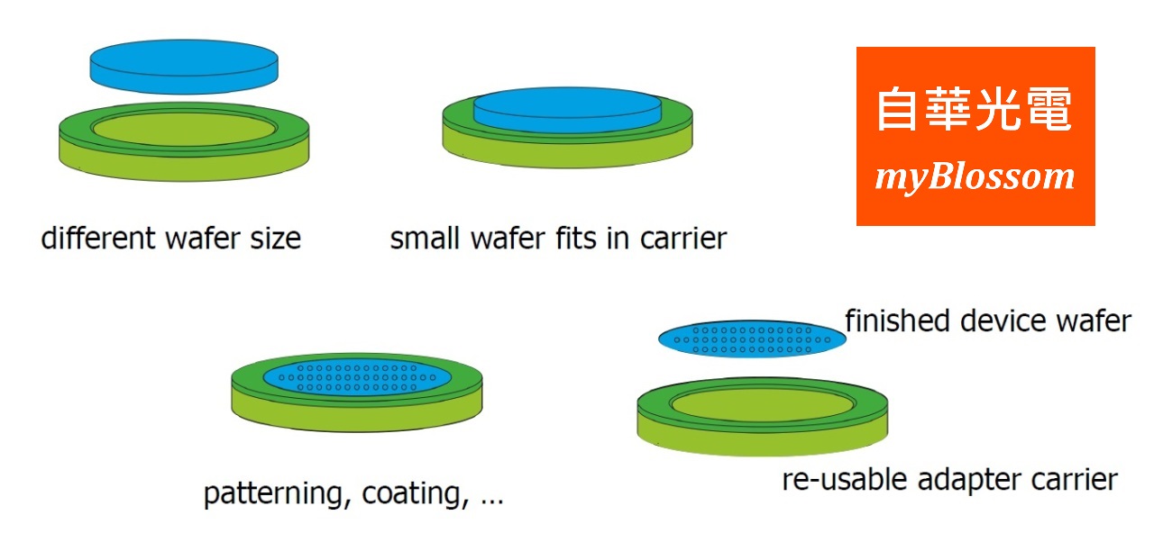
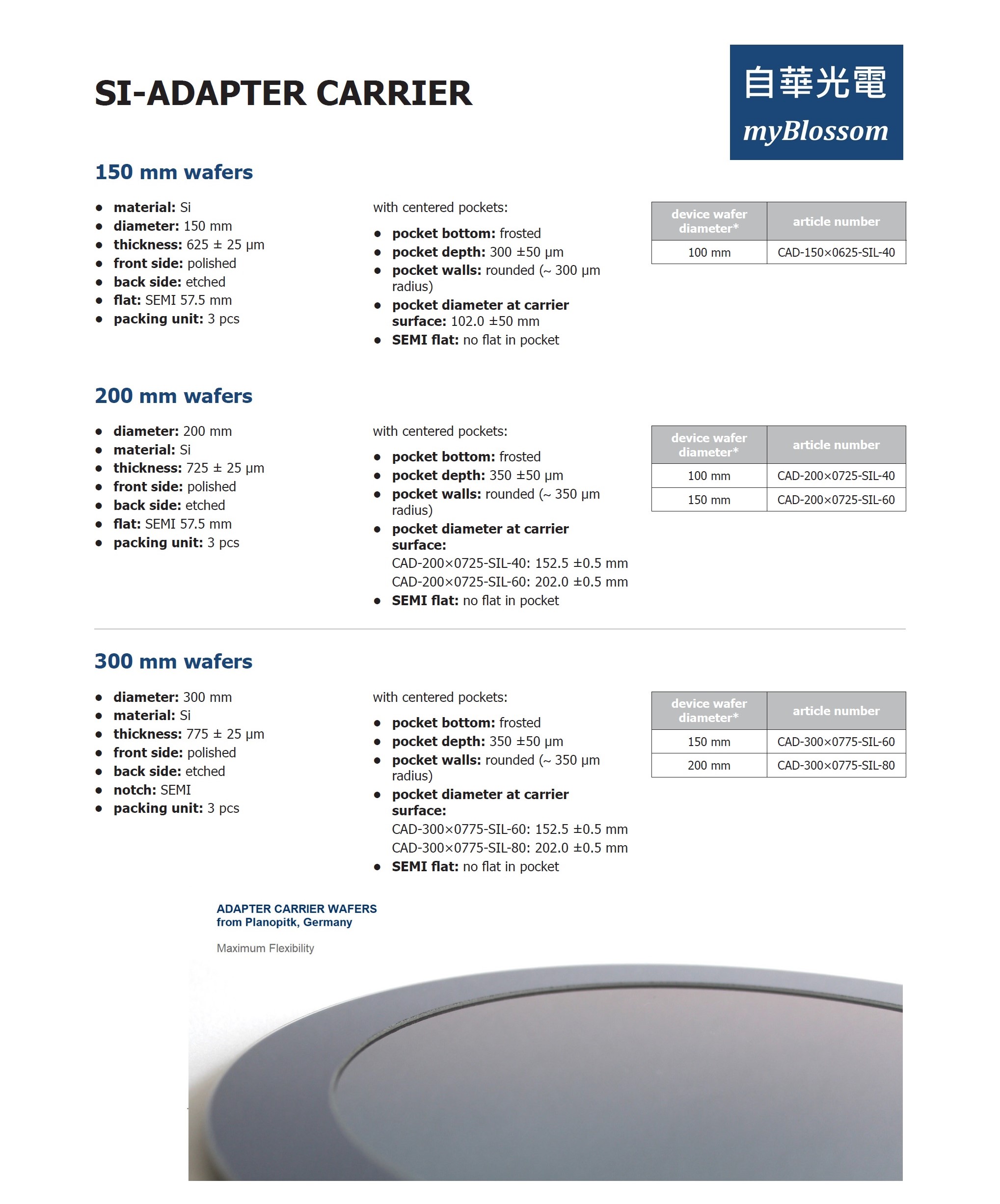
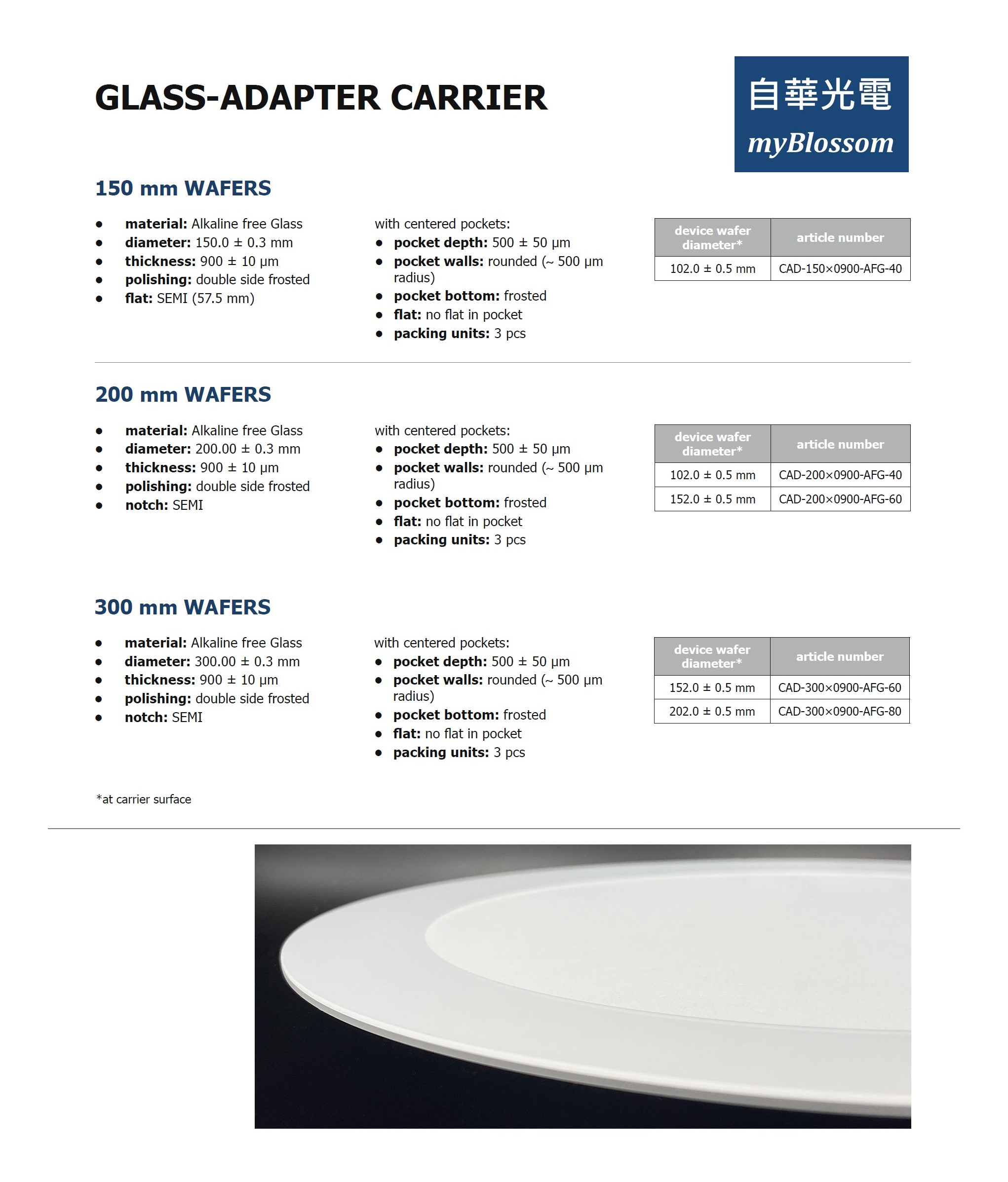
Adapter Carrier具有圖案化袋的單晶表面處理矽晶圓或永久黏合到硼矽酸鹽玻璃環上的矽晶圓,其已根據基板的尺寸圖案化。 晶圓上如此形成的口袋具有標準外徑,可以加工較小的晶圓和基板,例如200 mm設備上的150 mm晶圓或100 mm工具上的多個2“晶圓。
由於使用的材料,這些載體可以在最高500°C(~930°F)的工作溫度下使用。 此外可以添加孔或凹槽,以便能夠使用具有過程類型的Plan Optik適配器載體,例如真空安裝。
為了保證最高質量,Plan Optik採用了根據IATF 16949,ISO 14001和ISO 9001認證的質量管理體系。
Silicon Pocket Wafer / Silicon Adapter Carrier
----------------------------------------------------------------------------------
Glass Pocket Wafer / Glass Adapter Carrier
請索取適合您的工藝和產品要求的定制解決方案。
Adapter Carrier, Pocket Wafer, 晶圓載盤, 晶圓承載盤, 矽片承載盤

自華光電 - 德國Plan Optik AG 玻璃晶圓/石英晶圓 台灣獨家代理商。
Allen K. Lin | Allen@myblossom.tw | LINE ID: Allen-007 | Wechat ID: Allen-006 | T: 0910-782775

Adapter Carriers / Pocket Wafer - Maximum Flexibility
Adapter Carriers
Click here
Adapter Carriers / Pocket Wafer - Maximum Flexibility
Plan Optik AG offers Carrier Wafers which enable handling of smaller diameter wafers and a variety of substrates with different dimensions.
With increasing diameter of wafers processed in semiconductor industry not everyone can afford processing equipment or tools for different wafer diameter or even customized substrate dimensions.
Plan Optik‘s Adapter Carriers feature pockets to hold smaller dimension substrates or wafers with smaller diameter and carry them through the process - giving you the ability to handle and process a variety of different wafer and substrate sizes - on your existing equipment.
Adapter Carriers are either mono crystalline surface processed Silicon wafers with patterned pocket(s) or Silicon wafers permanently bonded to borosilicate glass rings that have been patterned according to the dimensions of substrate. The so formed pockets on the wafer with your standard outer diameter enables processing of smaller wafers and substrates as for example 150 mm wafers on 200 mm equipment or even multiple 2“ wafers on 100 mm tools.
Due to the materials used, these carriers can be used in operating temperatures up to 500°C (~930°F) max. In addition holes or grooves can be added to be able to use Plan Optik Adapter Carriers with process types as for example vacuum mounting.
In order to guarantee the highest quality, Plan Optik employs a quality management system certified as per IATF 16949, ISO 14001 and ISO 9001.
Please ask for a customized solution fitting to your process and product requirements.


