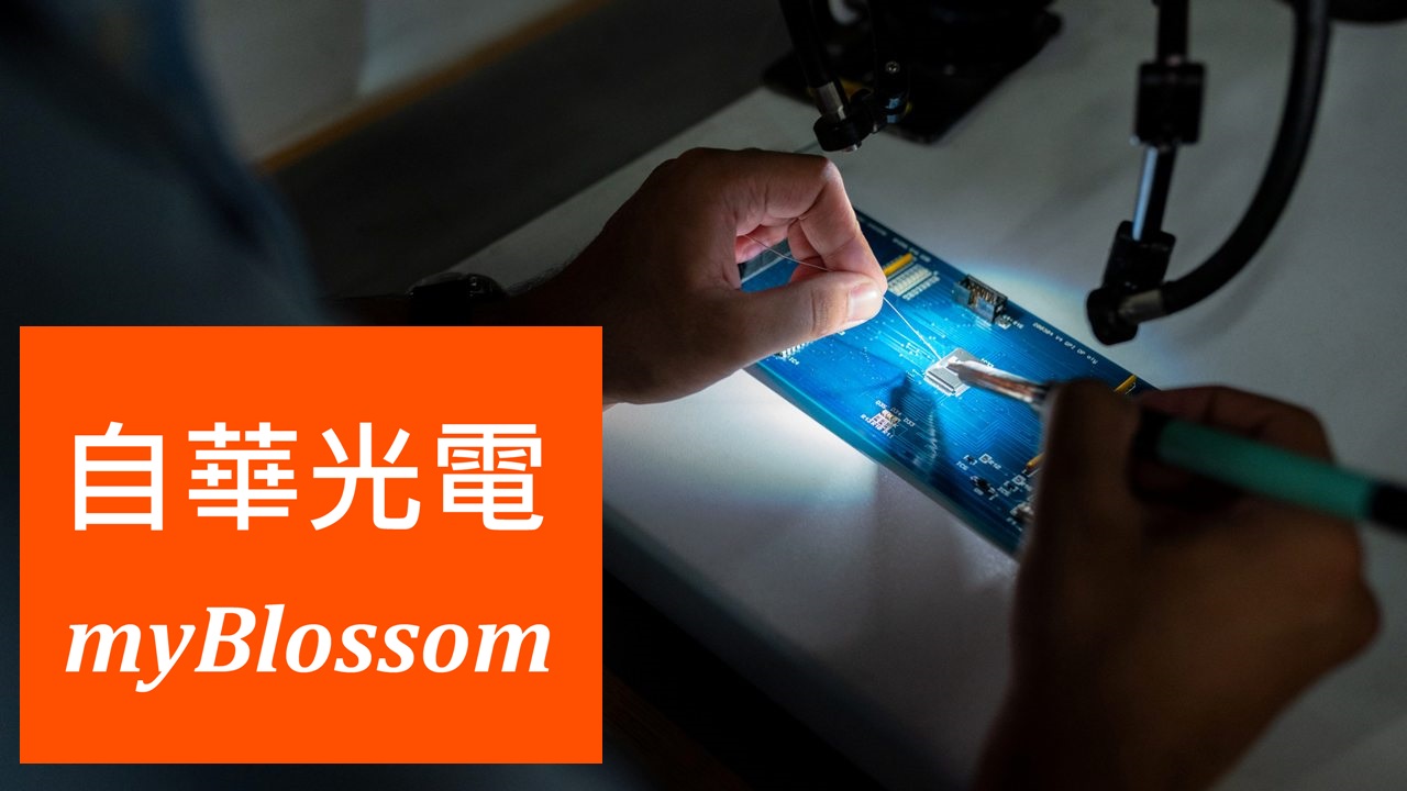
myBlossom® Cu-Interposer technology
Cu-Interposer
Click here 


myBlossom® Cu-Interposer technology
Plan Optik AG, the leading manufacturer of customized wafers from glass, quartz or glass-silicon compound materials has launched its new Cu-Interposer technology at SEMICON Europa 2019.
General properties
> patterned Wafer diameter from 2” up to 300 mm
> customized Redistribution Layers (RDL) up to 8″
> thickness from 200 µm to 1 mm
> wafers, panels or boards
> hole diameter from 100 µm (depending on wafer thickness)
> minimum pitch equal to via diameter
> Cu-layer thickness starting from 1 μm
The progressive miniaturization, increasing integration density and requirements for more powerful signal routing create the need for 3D integration. Interposer technologies for rewiring have been developed for efficient communication with high transmission rates in the 3D chip stack or 3D system package. At present, organic interposers are predominantly used for these technologies. Organic interposers can be produced inexpensively, but are no match for the modern and increasing demands on 3D integration and high transfer rates. Through Glass Via Wafers (TGVs) offer a cost-effective alternative to the costly silicon interposer technology. TGV interposers are a promising technology for three-dimensional and high-density hybrid integration. For high-frequency applications and optoelectronic components, insulation layers are integrated and therefore not required compared to silicon technology of IC chips.
But: There is no established solution to produce glass interposers at wafer level, which provides all the required properties for high-frequency applications. For this reason, Plan Optik has developed a new technology to produce interposers with an applied copper layer, which is particularly suitable for high-frequency applications.
Next Generation Interposer
As a first step, Plan Optik will be able to offer Interposers as drilled glass wafers with a copper layer. Those Interposer wafers will be available in sizes up to 300 mm with hole diameters down to 100 µm (depending on wafer thickness). At present, customized Redistribution Layers (RDL) can be integrated on wafer sizes up to 8”. The wafer thickness ranges from 200 µm up to 1 mm. Plan Optik’s Cu-Interposer can be produced as a wafer, as panels or as boards depending on customer needs. With a minimum hole distance equal to via diameter and a Cu-layer thickness starting from 1 µm Cu-Interposer are perfectly suitable for high-frequency applications like for example 5G broadband transmission, radar and imaging sensors, biosensors or beam steering networks.
More products coming soon
In the next steps Plan Optik will be able to add via fillings and pluggings to raise the device on the Interposer / Board as well as adding solder masks soon. Furthermore, Plan Optik’s latest interposer technology also paves the way for more exciting products and applications such as Glass-Circuit-Boards (GCB) with Integrated Passive Devices (IDP) like capacitors, resistors or coils as well as products with highest integration density, which will be used to realize antenna modules.

myBlossom® - Plan Optik® exclusive agent in Taiwan
The progressive miniaturization, increasing integration density and requirements for more powerful signal routing create the need for 3D integration. Interposer technologies for rewiring have been developed for efficient communication with high transmission rates in the 3D chip stack or 3D system package. At present, organic interposers are predominantly used for these technologies. Organic interposers can be produced inexpensively, but are no match for the modern and increasing demands on 3D integration and high transfer rates. Through Glass Via Wafers (TGVs) offer a cost-effective alternative to the costly silicon interposer technology. TGV interposers are a promising technology for three-dimensional and high-density hybrid integration. For high-frequency applications and optoelectronic components, insulation layers are integrated and therefore not required compared to silicon technology of IC chips.
But: There is no established solution to produce glass interposers at wafer level, which provides all the required properties for high-frequency applications. For this reason, Plan Optik has developed a new technology to produce interposers with an applied copper layer, which is particularly suitable for high-frequency applications.
Next Generation Interposer
As a first step, Plan Optik will be able to offer Interposers as drilled glass wafers with a copper layer. Those Interposer wafers will be available in sizes up to 300 mm with hole diameters down to 100 µm (depending on wafer thickness). At present, customized Redistribution Layers (RDL) can be integrated on wafer sizes up to 8”. The wafer thickness ranges from 200 µm up to 1 mm. Plan Optik’s Cu-Interposer can be produced as a wafer, as panels or as boards depending on customer needs. With a minimum hole distance equal to via diameter and a Cu-layer thickness starting from 1 µm Cu-Interposer are perfectly suitable for high-frequency applications like for example 5G broadband transmission, radar and imaging sensors, biosensors or beam steering networks.
More products coming soon
In the next steps Plan Optik will be able to add via fillings and pluggings to raise the device on the Interposer / Board as well as adding solder masks soon. Furthermore, Plan Optik’s latest interposer technology also paves the way for more exciting products and applications such as Glass-Circuit-Boards (GCB) with Integrated Passive Devices (IDP) like capacitors, resistors or coils as well as products with highest integration density, which will be used to realize antenna modules.

myBlossom® - Plan Optik® exclusive agent in Taiwan
Allen K. Lin | Allen@myblossom.tw | LINE ID: Allen-007 | WeChat ID: Allen-006 | T: 0910-782775


自華光電®Cu-Interposer技術 myBlossom® Cu-Interposer technology
Links
Click here 


自華光電®Cu-Interposer技術 myBlossom® Cu-Interposer technology
由玻璃,石英或玻璃-矽複合材料製成的定製晶圓的領先製造商Plan Optik AG在2019年SEMICON Europa上推出了其新的Cu-Interposer技術。
一般性質
>圖案化的晶圓直徑從2英寸到300毫米
>定制的重新分發層(RDL)高達8英寸
>厚度從200 µm到1 mm
>晶圓,面板或板
>孔徑從100 µm起(取決於晶片厚度)
>最小間距等於通孔直徑
>銅層厚度從1μm開始
逐步的小型化,集成密度的提高以及對更強大的信號路由的要求,導致了對3D集成的需求。已經開發出用於重新佈線的插入器技術,以在3D芯片堆棧或3D系統封裝中以高傳輸速率進行有效通信。目前,有機中介層主要用於這些技術。有機中介層的生產成本低廉,但與3D集成和高傳輸速率的現代和日益增長的需求不匹配。直通玻璃晶圓(TGV)提供了一種經濟高效的替代方案,可替代昂貴的矽中介層技術。 TGV中介層是用於三維高密度混合集成的有前途的技術。對於高頻應用和光電組件,絕緣層是集成的,因此與IC芯片的矽技術相比,不需要絕緣層。
但是:目前尚沒有成熟的解決方案來生產晶圓級的玻璃中介層,該解決方案提供了高頻應用所需的所有特性。由於這個原因,Plan Optik開發了一種新技術來生產具有鍍銅層的中介層,特別適合於高頻應用。
下一代Interposer
第一步,Plan Optik將能夠提供中介層,作為帶有銅層的鑽孔玻璃晶片。這些Interposer晶片的尺寸最大為300 mm,孔的直徑最小為100 µm(取決於晶片的厚度)。目前,定制的再分佈層(RDL)可以集成到最大8英寸的晶圓上。晶圓厚度範圍從200 µm到1 mm。 Plan Optik的Cu-Interposer可以根據客戶需求以晶片,面板或板的形式生產。最小的孔距等於通孔直徑,並且Cu層厚度從1 µm開始,非常適合高頻應用,例如5G寬帶傳輸,雷達和成像傳感器,生物傳感器或波束控製網絡。
更多產品即將推出
更多產品即將推出
在接下來的步驟中,Plan Optik將能夠通過填充物和塞子進行添加,以提高內插器/板上的設備的質量,並很快添加阻焊層。此外,Plan Optik的最新插入器技術還為更令人興奮的產品和應用鋪平了道路,例如帶有集成無源器件(IDP)的玻璃電路板(GCB),例如電容器,電阻器或線圈,以及具有最高集成密度的產品。將用於實現天線模塊。

自華光電® - 德國Plan Optik AG 玻璃晶圓/石英晶圓 台灣獨家代理商。

自華光電® - 德國Plan Optik AG 玻璃晶圓/石英晶圓 台灣獨家代理商。
Allen K. Lin | Allen@myblossom.tw | LINE ID: Allen-007 | WeChat ID: Allen-006 | T: 0910-782775


