自華光電®標準石英晶圓 myBlossom® Quartz Wafer


自華光電®標準石英晶圓 現貨超市
myBlossom® Quartz Wafer
自華光電®代理全球最大標準玻璃晶圓/石英晶圓現貨超市。
半導體級石英(非晶)晶圓用於半導體加工、太陽能和工業應用以及薄膜塗層。 主要特點是化學純度高,使其成為 CMOS 兼容材料,同時具有出色的機械和光學性能。
半導體級石英具有低 cte 和低 OH 含量,可實現高溫加工以及在 IR 和 UV 中的良好透射。 就價格合理的高質量石英晶片而言,這種材料是一流的。標準晶圓有常備庫存可現貨供應。
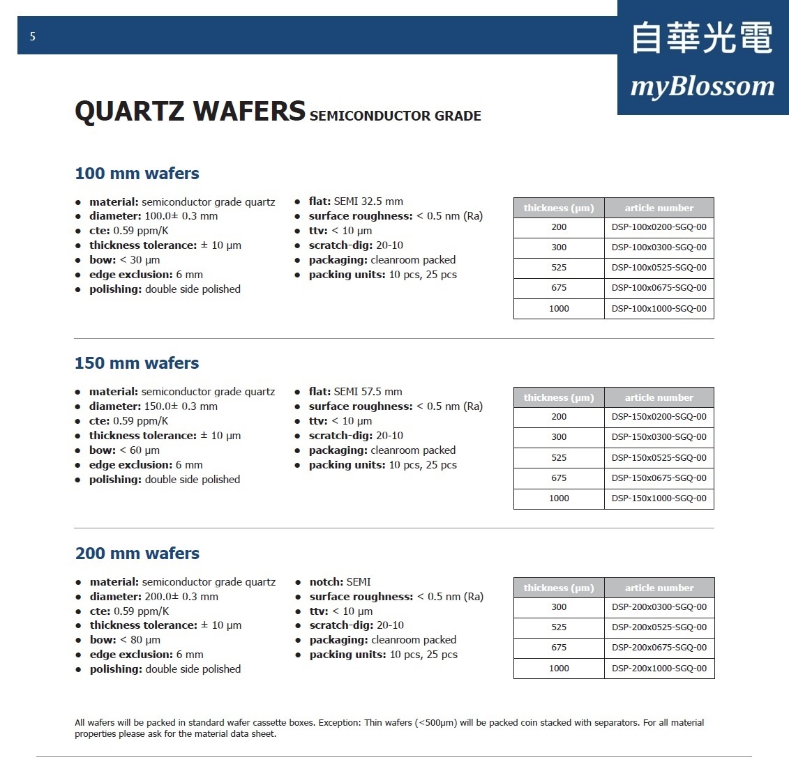 除了上述標準石英晶圓有現貨供應外,根據客戶的規格生產客製化石英晶圓(不同厚度,直徑與規格)。
自華光電 - 德國PlanOptik AG 玻璃晶圓/石英晶圓 台灣獨家代理商。
Allen K. Lin | Allen@myblossom.tw | LINE ID: Allen-007 | Wechat ID: Allen-006 | T: 0910-782775

myBlossom® Standard Quartz Wafer
myBlossom® Standard Quartz Wafer
Wafers from semiconductor grade quartz (amorphous) are used in semiconductor processing, solar and industrial applications as well as for thin film coatings. Main feature is the high chemical purity making it a CMOS compatible material combined with excellent mechanical and optical properties.
Semiconductor grade quartz features low cte as well as low OH content which enables high temperature processing and good transmission in IR and UV. This material is top notch when it comes to high quality quartz wafers with reasonable pricing.

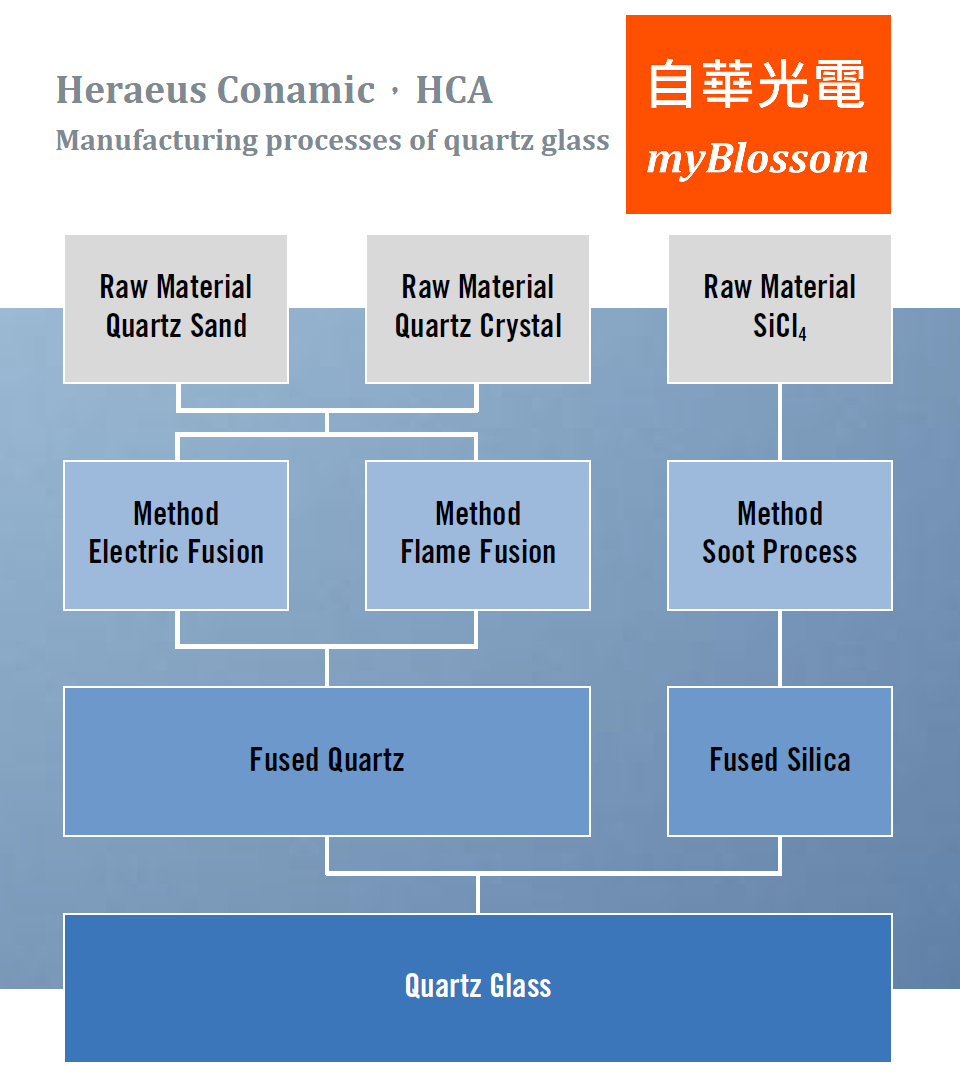
Heraeus Conamic,HCA
Heraeus Conamic is a technology leader and a leading-edge material specialist for the manufacturing and processing of the industry’s highest purity fused silica and other high-end materials such as ceramics and composites.
The organization excels in all key processes for producing natural fused quartz and synthetic fused silica for the semiconductor and photonics industry. Additionally, high-end materials like ceramics and composites are within our material focus. With locations all around the globe, Heraeus Conamic offers fused silica and ceramic products ranging from semi-finished goods to complex system components to custom-tailored solutions.
引述自Heraeus產品介紹

石英玻璃/Quartz glass, JGS1、JGS2、JGS3
石英玻璃/Quartz glass, JGS1、JGS2、JGS3
在光學元件中,中國石英玻璃按光譜應用範圍主要可分為JGS1、JGS2、JGS3三種型號:
JGS1 (遠紫外光學石英玻璃)
它是一種以SiCl 4為原料的人造石製成的光學石英玻璃,並通過高純度氫氧火焰熔化。因此它含有大量的羥基(約2000 ppm),並具有出色的紫外線透射性能。特別是在短波紫外線區域,其傳輸性能遠優於所有其他類型的玻璃。185nm處的紫外線透射率可以達到90%或更高。合成石英玻璃在2730nm處具有很強的吸收峰,並且沒有顆粒結構。它是185-2500nm範圍內的出色光學材料。
JGS2 (紫外光學石英玻璃)
它是通過以晶體為原料的氣體精製而成的石英玻璃,包含數十種PPM金屬雜質。在100nm處有吸收峰(羥基含量為200-2730ppm),具有條紋和顆粒結構。它是在220-2500nm波段範圍內的優良材料。
JGS3(紅外光學石英玻璃)
它是通過真空壓力爐(即電熔法)以晶體或高純石英砂為原料生產的石英玻璃,其中含有數十種PPM金屬雜質。但是它具有小的氣泡,顆粒結構和條紋,幾乎沒有OH,並且具有很高的紅外透射率。透光率超過85%。它的應用範圍是260-3500nm光學材料。
引述自MICQ產品介紹
與中國國產材料比較,我們提供Heraeus、Corning、Schott等主要製造商的等級和規格的材料。材料的純度高,均勻性好,生產出的晶圓產品性能更穩定。