自華光電®標準玻璃晶圓-超級拋光 myBlossom® Glass Wafer-MDF


自華光電®標準玻璃晶圓-超級拋光
myBlossom® Glass Wafer-MDF
自華光電®代理全球最大標準玻璃晶圓/石英晶圓現貨超市。
標準玻璃晶圓-超級拋光 採用德國Schott公司的BOROFLOAT 33玻璃材料。
MDF 拋光晶圓經過增強拋光工藝(Micro Damage Free, 無微損傷)處理。 這些晶圓專為化學圖案化工藝(濕法蝕刻)開發,由於缺陷率降低,產量更高。
它們極低的亞納米級表面粗糙度使它們非常適合直接鍵合(熔合鍵合)。
BOROFLOAT 33 = BOROFLOAT33 = BF 33 = BF33


myBlossom® Glass Wafer-MDF
myBlossom® Glass Wafer-MDF
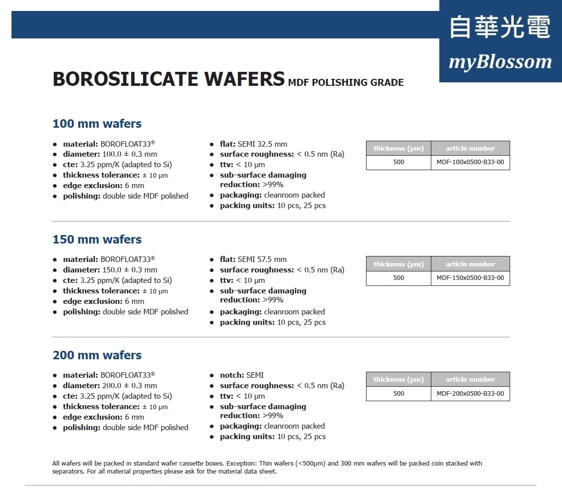
BOROSILICATE WAFERS MDF POLISHING GRADE
MDF polished wafers are treated by an enhanced polishing process (Micro Damage Free) developed by Plan Optik. These wafers are specifically developed for chemical patterning processes (wet-etching) leading to higher yield due to reduced defect rate. Their extremely low sub-nanometer surface roughness makes them ideally suited for direct bonding (fusion bonding).
MAIN PROPERTIES
• material: BOROFLOAT33®
• cte of 3.25 ppm/K (adapted to Si)
BOROFLOAT 33 , BOROFLOAT33 , BF 33 , BF33

BOROFLOAT® 33 和玻璃晶圓
BOROFLOAT® 33 和玻璃晶圓
20多年前,SCHOTT 建立了全球首條微浮法玻璃生產線,該條生產線的玻璃很快就成為全球有史以來最具影響力的玻璃產品之一。BOROFLOAT® 是全球首款硼矽浮法玻璃。以德國高品質工程技術為核心,加上專業團隊的開發動力,BOROFLOAT®迅速成為先進技術、創新工藝和專業性完美結合的傑出典範。
對於玻璃晶圓用於陽極鍵合或在晶圓減薄的製程中當成載體的性能要求,主要取決於它們能完全與矽晶圓作永久或暫時的黏合。和矽晶圓相當的熱膨脹係數,優異的平整度與製程的穩定性同等重要。BOROFLOAT® 玻璃晶圓提供如此卓越的材料特性以及超高的紫外線穿透性 - 可用於高速雷射脫黏製程中的特殊需求。BOROFLOAT® 玻璃完全與矽的熱膨脹係數一致,這是成功黏合所需的必要條件。在製程中晶圓時常曝露於溫度變動的環境下。低線性熱膨脹係數使得BOROFLOAT® 玻璃晶圓能輕易的應對升高的溫度,更重要的是,在突然的溫度變化下,不會發生破裂或翹曲。
BOROFLOAT® - 優異特性成就獨特的玻璃晶圓
• 卓越耐熱性能
• 特高透光度
• 高化學耐久性
• 優異的機械強度
以 BOROFLOAT® 玻璃作成的玻璃晶圓提供卓越的耐熱性能。BOROFLOAT® 玻璃完全與矽的熱膨脹係數一致,這是成功黏合所需的必要條件。在製程中晶圓時常曝露於溫度變動的環境下。低線性熱膨脹係數使得 BOROFLOAT® 玻璃晶圓能輕易的應對升高的溫度,更重要的是,在突然的溫度變化下,不會發生破裂或翹曲。
具有極佳透光率的載體晶圓能允許特殊的紫外線黏合。藉由玻璃載體晶圓的雷射脫黏,提供了最快速的脫黏時間,以及良好的性價比。在相關的雷射波長範圍中,深紫外線的穿透率,對於此種晶圓脫黏的可行性與效率是很重要的。透過使用 248 nm 或 308 nm 的準分子雷射照射可用於雷射脫黏。極低含鐵量的 BOROFLOAT® 玻璃在所需求的載體厚度 0.5 mm,顯示出在波長 308 nm 超過 90 % 的透光率,以及在波長 248 nm 仍然超過 35 % 的透光率,因此顯著優於其它超薄平板玻璃。
酸、鹼以及有機物質幾乎無法影響 BOROFLOAT® 玻璃晶圓的性能。卓越耐化學性是另一個主要特色 : 在高度複雜的蝕刻環境,以及化學機械研磨 (CMP) 的製程中,晶圓暴露在許多化學物質中。在某些技術上,以光罩為基礎的化學蝕刻技術,使用多種強烈腐蝕性的化學品,以創造精確的表面通道。其中 BOROFLOAT® 33的高化學耐久性是關鍵,能夠提供完美的結構設計以及無與倫比的精度來控制通道深度。
以 BOROFLOAT® 製成的玻璃晶圓因為它可靠的製程穩定度而脫穎而出。許多晶圓的微結構時常需要藉由超音波鑽孔,噴砂或是光蝕刻和乾式蝕刻而製成。為了生產高精度且有著數以千計精準加工特徵的晶圓,製程中的機械強度和穩定性是極為重要的,特別是為了製造完美的表面圖案和準確的尺寸。BOROFLOAT® 玻璃相較於其它玻璃基板,具有極度耐磨的特性。
引述自Schott產品介紹

BOROFLOAT® 33 & Glass Wafers
BOROFLOAT® 33 & Glass Wafers
More than 20 years ago, SCHOTT set up the first micro-float production line for what would soon become one of the most influential specialty glass materials. The result was BOROFLOAT® – the world’s first floated borosilicate glass. With high-quality German engineering at its core, BOROFLOAT® quickly became an outstanding example of what seamless interaction between advanced know-how, innovative technology and professional curiosity – all in combination with the developmental drive of our team of experts – can deliver.
The performance requirements for glass wafers used for anodic bonding or as carrier wafers in wafer thinning processes are mainly determined by their ability to perfectly match those of the silicon wafer to which they shall be permanently or temporarily bonded. Well-adapted thermal expansion behaviour is as important as excellent flatness and process robustness. BOROFLOAT® glass wafers provide such outstanding material properties along with exceptionally high UV transmission – a special requirement for high speed laser de-bonding processes.
BOROFLOAT® - The sum of its properties is what makes it unique for glass wafers
• Outstanding thermal resistance
• Exceptionally high transparency
• High chemical durability
• Excellent mechanical strength
Glass wafers made of BOROFLOAT® glass offer outstanding thermal resistance. The glass composition of BOROFLOAT® is tailored to perfectly match the thermal expansion coefficient of silicon which is essential for good bonding behavior. Wafers are often exposed to thermally changing environments during processing. The low coefficient of linear thermal expansion (C.T.E.) allows BOROFLOAT® glass wafers to easily handle elevated temperatures and – often even more importantly - sudden thermal changes without breaking or warping.
Carrier wafers with unmatched light transmission allow for exceptional UV bonding. Laser de-bonding through glass carrier wafers offers the fastest de-bonding time as well as a good price / performance ratio. Deep UV light transmission at the relevant laser wavelength range is crucial for the principal feasibility and efficiency of this type of wafer de-bonding. The laseractivated release will be achieved through irradiation using a 248 nm or 308 nm excimer laser. Extra-low iron BOROFLOAT® glass of desirable 0.5 mm carrier thickness shows over 90 % transmission at 308 nm and still over 35 % for 248 nm, thus significantly outperforming other thin flat glasses.
Acids, alkalis and organic substances have virtually no negative impact on BOROFLOAT® glass wafers. Outstanding chemical resistance is another critical feature given that wafers are exposed to many chemicals throughout the highly sophisticated etching and chemical mechanical planarization (CMP) processes. In certain technologies, mask-based chemical etching technologies using an aggressive cocktail of corrosive chemicals are also applied in order to create high definition surface channels where the high chemical durability of BOROFLOAT® 33 is key to deliver perfectly shaped design structures of unmatched accuracy with controlled channel depth.
Glass wafers made of BOROFLOAT® stand out for their reliable process robustness. Many wafers require microstructures which are often created via ultrasonic drilling, powder blasting or a combination of photolithography and dry etching. Mechanical strength and stability during a process where thousands of accurate features have to be machined are essential in order to produce high precision textured wafers with a consistently perfect surface pattern and accurate size. BOROFLOAT® glass has an exceptional abrasion resistance compared to other alternative substrates.
Quoted from Schott Product Introduction