Home ﹥ Products > SoG晶圓|GoS晶圓

自華光電®矽玻璃晶圓 myBlossom® Silicon-on-Glass Wafer
自華®標準SoG晶圓 常備庫存明細
Click here 

自華光電®標準SoG晶圓 現貨超市
myBlossom® SoG Wafer
自華光電®代理全球最大標準玻璃晶圓/石英晶圓現貨超市。
自華光電®矽玻璃晶圓, 矽玻璃鍵合的晶圓, SoG晶圓
myBlossom® Silicon-on-Glass Wafer, SoG Wafer
自華光電®玻璃矽晶圓, 玻璃矽鍵合的晶圓, GoS晶圓
myBlossom® Glass-on-Silicon Wafer, GoS Wafer
SoG晶圓可使用於多種 MEMS 應用。這些晶圓會被客戶使用多種加工方式進一步加工成各種結構及其他 MEMS 的生產流程。
在這個 SOG晶圓/GOS晶圓,標準玻璃和矽晶圓是透過陽極鍵合的方式形成不可逆的鍵合層。單邊或是雙邊的晶圓複合體可透過使用材料本身所適合的 CMP 製程來研磨減薄到指定的厚度。這些製程所使用的玻璃晶圓是由我們生產,矽晶圓則使用市場上知名的廠商所生產常用的單晶矽標準晶圓。
整個晶圓的整體厚度最小可以做到 250 µm,而個別層(玻璃或矽)可以減薄到大約接近 20 µm。GOS 與 SOG 晶圓的邊緣進行特殊邊緣研磨,故可以去除掉鍵合時鍵合的間隙且不會減少晶圓的直徑,透過這個工藝可以減少所有的負面效應(粉塵汙染,破片的風險,操作的問題)。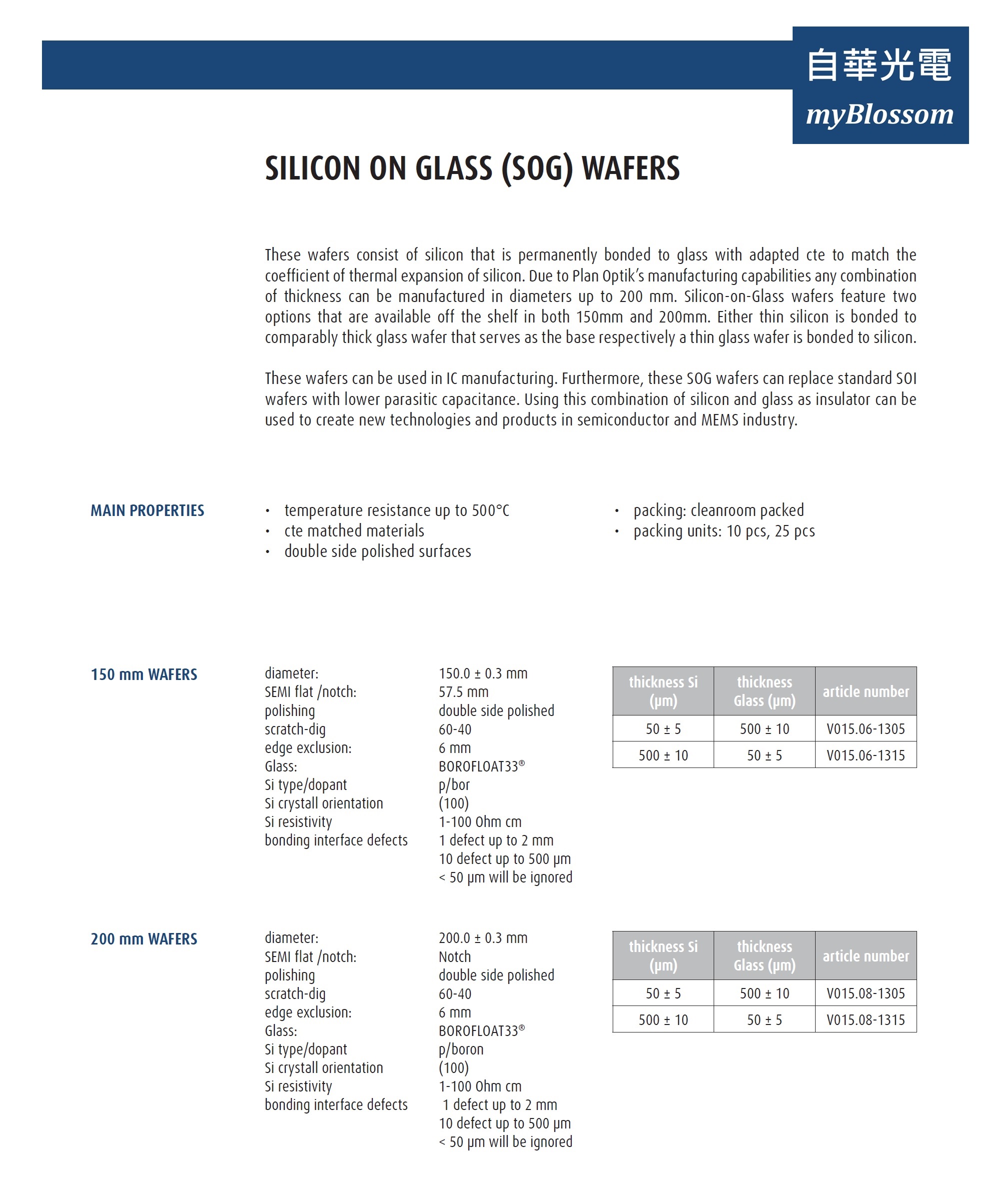
我們可以根據客戶的規格生產 GOS 的和 SOG 晶圓。
作為 MEMS 蓋板晶圓的基板並可以做到相當薄的玻璃厚度(如 50 µm),可與標準的矽晶圓基板搭配使用(如 500 µm)。
使用於 MEMS 光學產品做為蓋板,使矽晶圓部分區域在後製程可以被去除後形成透光區,例如使用氫氧化鉀(KOH)蝕刻來製造蓋板。

自華光電 - 德國Plan Optik AG 玻璃晶圓/石英晶圓 台灣獨家代理商。
Allen K. Lin | Allen@myblossom.tw | LINE ID: Allen-007 | Wechat ID: Allen-006 | T: 0910-782775
作為 MEMS 蓋板晶圓的基板並可以做到相當薄的玻璃厚度(如 50 µm),可與標準的矽晶圓基板搭配使用(如 500 µm)。
使用於 MEMS 光學產品做為蓋板,使矽晶圓部分區域在後製程可以被去除後形成透光區,例如使用氫氧化鉀(KOH)蝕刻來製造蓋板。

自華光電 - 德國Plan Optik AG 玻璃晶圓/石英晶圓 台灣獨家代理商。
Allen K. Lin | Allen@myblossom.tw | LINE ID: Allen-007 | Wechat ID: Allen-006 | T: 0910-782775


myBlossom® Silicon-on-Glass Wafer, SoG Wafer
SoG Wafer list
Click here
myBlossom® Silicon-on-Glass Wafer, SoG Wafer
myBlossom® Glass-on-Silicon Wafer, GoS Wafer
We offer these bonded wafers as a basic substrate for various MEMS applications. These wafers are then further processed by its customers using various structuring steps and other MEMS production processes.
In the case of GOS / SOG wafers, standard glass and silicon wafers are irreversibly bonded to each other by means of anodic bonding. One or both sides of the wafer stack can then subsequently be back thinned to the specified final thickness in each case using grinding and CMP processes adapted to the materials in question. The glass wafers employed are base wafers produced by Plan Optik itself, while the silicon wafers are widely available monocrystalline standard wafers by reputable manufacturers.
The minimum overall thickness of the entire wafer is about 250 µm, while the individual layers (glass or Si) can be thinned down by up to approx. 20 µm.
The edges of the GOS and SOG wafers have a special edge grind, which removes the bondgap which results during bonding without reducing the diameter of the wafer. In this way all negative effects (contamination through particles, danger of breaking, handling problems) are eliminated.
We manufactures GOS and SOG wafers according to customer specifications.

How glass and silicon team up to create paper-thin wafers for future gadgets
Glass on Web
Click here
How glass and silicon team up to create paper-thin wafers for future gadgets
Bacon and eggs. Batman and Robin. Ben and Jerry. BOROFLOAT® and silicon. It’s easy to spot perfect pairs.
Silicon wafers and BOROFLOAT® glass are one such duo, thanks to a unique set of characteristics that make these materials the ideal solution for caps on LED, MEMS, optical parts, and microfluidic device seals. As electronic circuits shrink to accommodate advancing smartphone cameras, car sensors, hologram projectors, and high-tech glasses, paper-thin wafers will act as the backbone to the integrated circuits that supply computing power.
Together, these two substrates act as essential players in the gadgets of today and of the future. Here’s how.
The incredible shrinking — and growing — wafer
The march toward circuit miniaturization presses on. Small, lightweight consumer devices rely on 3D circuit architecture built onto ultra-thin silicon wafers in order to perform at peak capacity. These wafers are extremely flat, with possible thickness deviations less than one micron. To achieve these razor-thin dimensions, glass wafers, especially SCHOTT’s borosilicate flat glass BOROFLOAT®, can act as a so-called “carrier wafer” in order to add precision and process stability during production.
These carrier wafers provide flat support during the manufacturing of ultra-thin silicon wafers. During manufacturing, these two wafers are temporarily bonded in order to smooth the silicon to a foil-like thickness. This process creates a surface free from imperfections and increases yields at a reduced cost. Once the process is complete, UV laser de-bonding separates the two substrates, leaving behind a silicon wafer just 50 microns thick.
At the same time, larger wafers, with a diameter of up to 12 inches, represent a new trend in wafer technology. As the wafer size increases in diameter, so does the efficiency of the network of integrated circuits. But to achieve that size, the substrate materials — glass especially — must maintain an extremely flat surface and offer superior process stability. The strength and flatness that can be achieved with a high-grade glass like BOROFLOAT® allow these wafers to reach diameters of up to a foot and growing.
The perfect match of materials
The quality of anodic bonding for MEMS and other electronic circuitry places the utmost demand on precision, and the threat of a hairline crack, warped wafer, or uneven surface creates pressure for perfection.
In MEMS applications, glass and silicon play well together — their thermal expansion coefficients are perfectly matched, so they behave nearly the same expansion behavior during processing. This quality ensures proper, gap-free anodic bonding, and its low coefficient of linear thermal expansion allows BOROFLOAT® to handle elevated temperatures without breaking or distorting.
In some applications, high-definition microstructure channels are etched into the substrate to create so-called “labs on a chip.” Throughout the etching and chemical polarization processes, the wafer is exposed to many chemicals that can degrade the substrate materials.
BOROFLOAT® solves this problem in two ways. First, the mechanical strength and stability of BOROFLOAT® ensure these patterns are precisely etched onto the substrate without it breaking. Next, the glass’ chemical properties ensure it won’t degrade, weaken, or react uncontrolled with these chemical cocktails.
Strong alone, but better together
Silicon has been the heart of the semiconductor industry since the 1960s, and glass wafers have become supplementary players over the past decade. Because semiconductor applications require flat, rigid materials that can withstand the pressures of manufacturing, glass substrates have grown in MEMS cap uses, as well as other electronic sensors and devices.
BOROFLOAT®, a high-grade glass with strong thermal, chemical, and mechanical properties, has become a partner to silicon in these ever-shrinking devices. BOROFLOAT® and silicon wafers can be precisely anodically bonded for certain MEMS applications, and it can act as a carrier wafer for specific silicon wafer applications featuring 3D architecture. The glass’ chemical composition, perfectly flat surface, and rigid structure provide an ideal complement to silicon in these semiconductor applications.
Tina Gallo, Manager, Applications and Logistic Services for SCHOTT's Home Tech division


