Home ﹥ Products > TGV|玻璃通孔晶圓

自華光電®玻璃通孔玻璃晶圓 myBlossom® Through Glass Vias (TGV) Wafer


自華光電®玻璃通孔(TGV)玻璃晶圓
myBlossom® Through Glass Vias (TGV) Wafer
自華光電®代理全球最大標準玻璃晶圓/石英晶圓現貨超市。
myBlossom透過使用專利的製程來生產導電穿孔晶圓,它讓玻璃與矽結合形成一個晶圓。這些具有高氣密性(真空)緊密結構的硼矽酸玻璃以及市面上可取得的所有種類矽可以單一晶圓上不受限地形成如繁星般的緊密分佈結構。透過使用與矽熱膨脹係數相近的硼矽酸玻璃,myBlossom的晶圓使用於 3D MEMS 的晶圓級封裝,藉以將封裝晶圓基板組成成可能具有力學,光學和電氣功能的結合體。這結果使得真空密封的蓋板晶圓也可在嚴苛的環境中所使用,例如在具有較高的溫度變化或濕度的環境。透過使用 myBlossom 的技術,可以讓多種功能結合並製成相對較小封裝尺寸的優點。
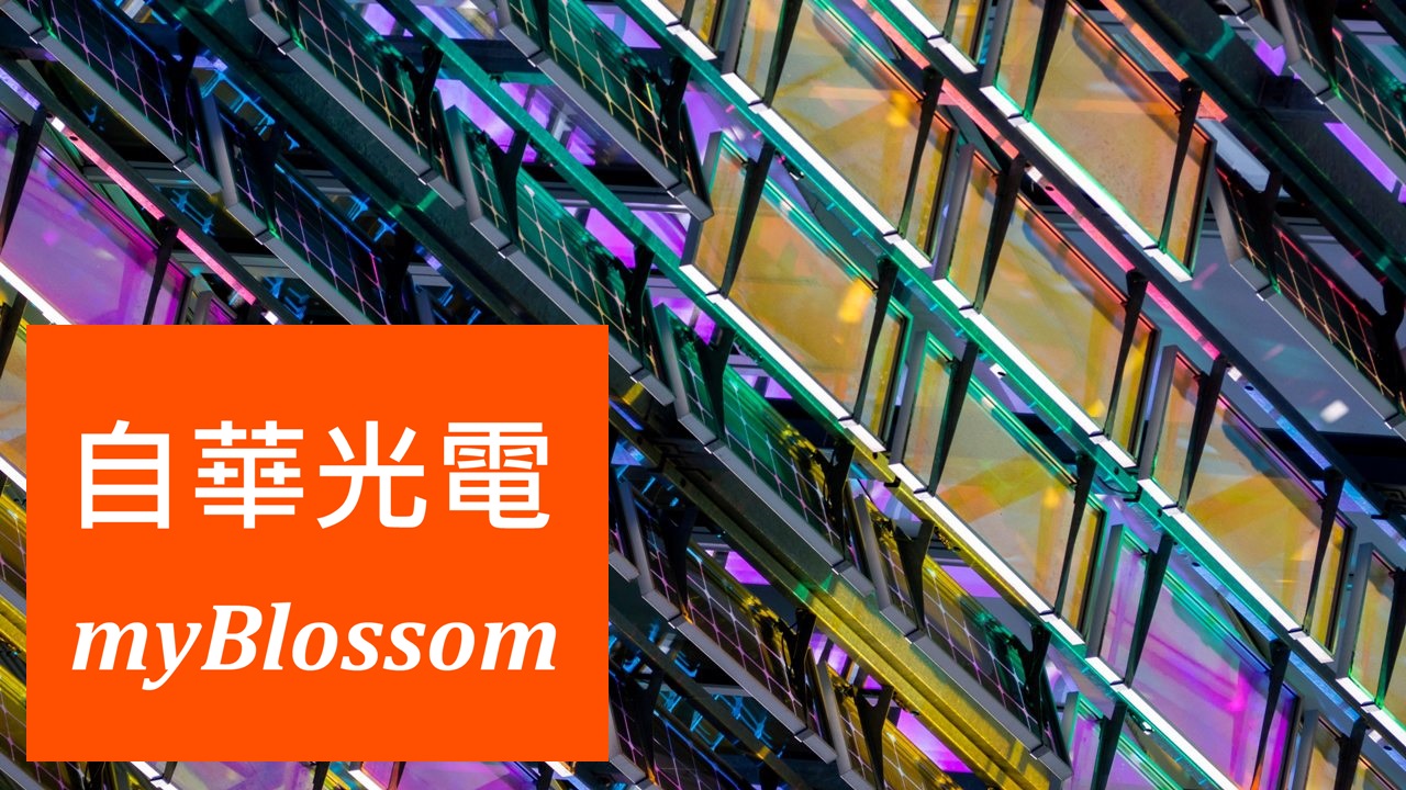
穿孔玻璃(TGV)玻璃晶圓 Through Glass Vias (TGV) Wafer
導通孔(TGV)玻璃晶圓 Through Glass Vias (TGV) Wafer

Allen K. Lin | Allen@myblossom.tw | LINE ID: Allen-007 | Wechat ID: Allen-006 | T: 0910-782775

VLIS process (short for Volume Laser Induced Structuring)
Plan Optik AG (Elsoff, Germany) and 4JET microtech (Alsdorf, Germany) have jointly developed a process chain for the highly productive production of metallized through-glass vias.
The new VLIS process (short for Volume Laser Induced Structuring) enables the production of high-precision TGV ("Through Glass Vias") for advanced packaging in glass wafers, or substrates for displays.
TGV are micro-holes with a diameter of typically 10µm to 100µm. For various applications in the advanced packaging sector, tens of thousands of these vias are applied per wafer and metallized to produce the required conductivity. TGV's are also used in the manufacture of borderless displays, for example based on µLED. Previous methods for manufacturing were slow, associated with high reject rates and difficult to match to the metallization process.
The teams from both companies have now developed a solution that can prepare several 10,000 vias per minute, which are etched in a subsequent batch process to be coated afterwards. The resulting channels are positioned with a hole-to-hole accuracy better than +/- 2µm. The substrates are free of microcracks, and the insides of the channels are smooth-walled and can be homogeneously metallized. The process is suitable for glass types typical in the semiconductor and display industry. In addition to glass starting thicknesses of 100µm, various copper layers down to 25µm thickness can be realized.
The two partners have agreed on a cooperation that provides users with a high degree of flexibility: Customers can either purchase components produced with VLIS from Plan Optik, or purchase qualified total solutions for system technology including laser systems, wet chemistry and metallization from 4JET and partners.
Plan Optik already has a modern production chain for the manufacture of glass wafers and masters all process steps from wafer cutting and edge processing, through structuring and cleaning, to metallization. The addition of 4JET's system technology now enables the rapid and positionally accurate modification of substrates. A modified version of the proven 4JET laser systems for cutting glass is used. The PEARL platform is already used for cutting glass substrates in display, architectural glass, or medical technology. Depending on the version, the systems are capable of high-precision modification of glass up to 2.2 m wide and more than 3 m long.
A new technology
The use of laser technology for selective etching is not new, but overall the cooperation delivers significant advances for customers: the combination with Plan Optik AG's extensive process chain creates the world's leading solution chain for fully processed and metallized TGV wafers. At the same time, the precision, speed and availability now achievable on very large substrates enables application in display manufacturing for the first time.
The two partners see further potential for the VLIS process for glass-based MEMS, microfluidics or high-frequency antenna technology (e.g. 6G).
The PEARL systems are based on a granite machine platform that offers inherent accuracy and long-term stability. Cutting geometries and positions for interposers can be easily imported from CAD drawings. Targeted tuning of axis controls results not only in high cutting speed, but also in excellent path accuracy to achieve high-precision machining. The PEARL DYNAMIC FOCUS ensures that the focus is always within the process window without increasing the process time.

myBlossom® Through Glass Vias (TGV)
myBlossom® Through Glass Vias (TGV)
We manufacture TGV using a patented process which permits the combination of glass and silicon within a single wafer. These hermetically (vacuum-) tight structures of borosilicate glass and all varieties of silicon generally available on the market can be distributed in virtually unlimited ratios and geometric constellations within a single wafer.
Through the use of borosilicate glass with a thermal expansion coefficient adapted to that of silicon, these wafers are used in 3D wafer level packaging of MEMS, whereby the combination of mechanical, optical and electrical functions within a packaging wafer substrate is made possible. This results in vacuum-tight cap wafers which can also be used in demanding environments, for example with high temperature fluctuations or humidity. The advantage of the combination of several functions lies in a relatively small package size through the use of advanced technology.