
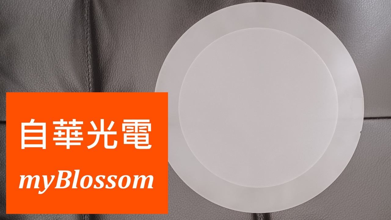
自華光電®封裝晶圓 myBlossom® Packaging Wafer
石英晶圓/玻璃晶圓 現貨超市
Click here 
自華光電®代理全球最大石英晶圓|玻璃晶圓 現貨超市。
自華光電®所代理的封裝晶圓包含客製化的石英晶圓/玻璃晶圓,或是組合玻璃、石英與矽這三種材料的複合晶圓。晶圓直徑從50mm到300mm,具有低厚度公差與低 TTV 值。在每個應用上根據客戶特定的要求加工晶圓表面的結構,例如光學腔體、鍍膜與鑽孔。
自華光電®所代理的封裝晶圓用來封裝並應用在高氣密性要求的光學或是化學偵測器、壓力傳感器與加速度傳感器。典型的產業應用在消費性電子產品(CMOS影像,微反射鏡)、汽車工業(壓力傳感器,如輪胎、發動機監控)、航空(三維加速度傳感器)、化學(微反應技術)、醫藥(實驗室晶片)以及一般的半導體製造。

自華光電® - 德國PlanOptik AG 玻璃晶圓/石英晶圓 台灣獨家代理商(from 2016/05/01) & 大陸獨家代理商(from 2021/06/01)。
Allen K. Lin | Allen@myblossom.tw | LINE ID: Allen-007 | WeChat ID: Allen-006 | T: 0910-782775
--------------------------------------------------------------------------------------------------------
玻璃材料(Borofloat 33 & Eagle XG)採購自Schott & Corning。

Packaging Wafers
Packaging Wafers, from Plan Optik AG
Click here
We manufacture packaging wafers from custom-made single items to large-scale series using glass, quartz and silicon and combinations of these three materials. The diameter is 50 - 300 mm with low thickness tolerances and low ttv values. In each case the structuring of the wafer is carried out on a customer-specific basis, for example with optical cavities, coatings and drillings.
Packaging wafers are used to pack and thus to seal hermetically optical or chemical sensors, pressure sensors and acceleration sensors. Typical industrial applications lie in the fields of consumer electronics (CMOS imaging, micro-mirrors), automotive technology (pressure sensors, e.g. tires, engine monitoring), aerospace (3D acceleration sensors), chemistry (micro-reaction technology), pharmaceuticals (lab-on-chip) and in the general manufacture of semiconductors.
Packaging wafers are used to pack and thus to seal hermetically optical or chemical sensors, pressure sensors and acceleration sensors. Typical industrial applications lie in the fields of consumer electronics (CMOS imaging, micro-mirrors), automotive technology (pressure sensors, e.g. tires, engine monitoring), aerospace (3D acceleration sensors), chemistry (micro-reaction technology), pharmaceuticals (lab-on-chip) and in the general manufacture of semiconductors.

Glass Wafers
Substrate Wafers, from Plan Optik AG
Click here
Standard wafers are available at short notice ex warehouse (subject to prior sales). Standard wafers are available either with the established standard polish finish - or with the enhanced MDF polish finish with minimized micro damaging at wet etching and acid cleaning processes.
We produces customized wafers from various types of glass and quartz, from single-item production to large-scale series. The diameter measures between 50 - 300 mm with low thickness tolerances and low ttv values.
Customized wafers are used to manufacture optical or chemical sensors, pressure sensors and acceleration sensors. Typical industrial areas of application lie in the consumer electronics sector (CMOS imaging, micro mirrors), automotive sector (pressure sensors, e.g. tires, engine control), aerospace (3D acceleration sensors), chemistry (micro reaction technology), pharmaceuticals (Lab-on-chip) and in semiconductor production in general.
** Glass Wafer materials
Schott: D263T eco , AF32 eco , MEMpax , BOROFLOAT 33 , B270 , FOTURAN II , AS87 eco , 0787 , BF33 , D263
Corning: SG3.4 , SG7.8 , SG9.0 , SG-HS , SG-HC , Eagle XG , EXG , EagleXG , SGW3 , SGW7.6 , SGW8 , SGW8.5 , SG8.4 , SG8.7
NEG: ABC-G , A58 , A66S , A69 , A75 , A91S
AGC: EN-A1

Quartz Wafers
Quartz Wafers, from Plan Optik AG
Click here
QUARTZ WAFERS OFF THE SHELF
In urgent need of quartz wafers? You order - we ship off the shelf (subject to availability and prior sales). Minimum order quantity: just 10 pieces.
Made from amorphous silicon dioxide of high purity. It provides a very good transmission in the near UV, VIS and IR wavelength region. The thermal expansion as well as the OH content is very low which makes them suitable for almost all application in near UV, VIS and IR - especially for high temperature applications. Wafers from this material are virtually bubble and fluorescence free.
CUSTOMIZED QUARTZ WAFERS
Besides quartz wafers, which are available off the shelf, we manufacture quartz wafers (SiO2) in a large scale production using high purity quartz glass. In contrast to crystalline quartz, the substance used here is amorphous quartz glass. These wafers are characterized by low thickness tolerances, high quality surfaces and low ttv values.
Our quartz wafers are defined as an alkaline-free and ultra-pure substrate, virtually unadulterated by foreign matter. They are therefore used in semiconductor technology and as a coating substrate. Typical industrial fields of application include the construction of RF modules, PLC splitters as well as micro fluidics and medicine. Our quartz wafers are resistant to high temperatures and virtually non-fluorescent.
** Quartz Wafer Materials:
Heraeus Conamic, Quartz Glass Plates
* Electrically fused quartz: HSQ 300 , HSQ 330 , OM 100
* Flame fused quartz: TSC-3 , TSC-4
* Synthetic fused silica: HSQ 900 , Spectrosil 1000
Corning Fused Silica: HPFS 7979 , HPFS 7980 , HPFS 8655
China Grade: JGS1 , JGS2 , JGS3


Silicon On Glass wafers / Glass On Silicon wafers
SOG & GOS wafers, from Plan Optik AG
Click here
GLASS ON SILICON / SILICON ON GLASS WAFERS
We offer these bonded wafers as a basic substrate for various MEMS applications. These wafers are then further processed by its customers using various structuring steps and other MEMS production processes.
In the case of GOS / SOG wafers, standard glass and silicon wafers are irreversibly bonded to each other by means of anodic bonding. One or both sides of the wafer stack can then subsequently be back thinned to the specified final thickness in each case using grinding and CMP processes adapted to the materials in question. The glass wafers employed are base wafers produced by Plan Optik itself, while the silicon wafers are widely available monocrystalline standard wafers by reputable manufacturers.
The minimum overall thickness of the entire wafer is about 250 µm, while the individual layers (glass or Si) can be thinned down by up to approx. 20 µm. The edges of the GOS and SOG wafers produced by Plan Optik have a special edge grind, which removes the bondgap which results during bonding without reducing the diameter of the wafer. In this way all negative effects (contamination through particles, danger of breaking, handling problems) are eliminated. Plan Optik manufactures GOS and SOG wafers according to customer specifications.


